Making RiscyOS: I SPI an SD Card
In this post, I dive into the design and implementation of an SPI-based SD card interface for RiscyOS. I walk through building a Verilog SPI peripheral and my own debugging experience.
This is part two of my RiscyOS development blog. In this part I outline the process of creating a SPI peripheral for communicating with an SD card.
For reference the breakout board that I bought was: Adafruit SD 3V Breakout Board.
An SD card uses two main communication protocols, Serial Peripheral Interface (SPI) and Secure Digital Input Output (SDIO). SDIO was introduced in 2001 and is generally faster because it allows for a higher clock rate (50MHz for SDIO vs 40MHz for SPI) and has four data pins (DAT0-3) and allows for 4 bits to be transferred in comparison to SPI which only has MISO and MOSI and allows for 1 bit of transfer.
Despite SDIO being faster and having a higher bandwidth is not as well documented as SPI, is more complex to implement and is not universally supported. For these reasons I chose to use SPI.
I had two options either bit-bang or create a dedicated peripheral which deals with it in hardware. Lets analyse these two options
My hardware runs at 40MHz and to bit bang spi the general sequence would be:
; a0 = byte to transmit
; a0 = byte received

transfer_byte:
    la   t0, SPI_GPIO        ; GPIO register
    li   t1, 7               ; bit index
    li   t4, 0               ; received byte

loop:
    # Get transmit bit
    srl  t2, a0, t1
    andi t2, t2, 1

    # Set MOSI
    lw   t3, 0[t0]
    li   t5, MOSI_BIT
    not  t6, t5
    and  t3, t3, t6          ; clear MOSI
    beqz t2, f1
    or   t3, t3, t5          ; set MOSI if bit=1
1:
    sw   t3, 0[t0]

    # Clock high
    ori  t3, t3, SCK_BIT
    sw   t3, 0[t0]

    # Sample MISO
    lw   t3, 0[t0]
    andi t3, t3, MISO_BIT
    beqz t3, 2f
    li   t5, 1
    sll  t5, t5, t1
    or   t4, t4, t5
2:

    # Clock low
    lw   t3, 0[t0]
    li   t5, SCK_BIT
    not  t6, t5
    and  t3, t3, t6
    sw   t3, 0[t0]

    addi t1, t1, -1
    bgez t1, loop

    mv   a0, t4
    ret
I know this code is not optimised but it serves as a demonstration of what a bit-banged SPI would look like and from my calculations the worst case scenario (where we send 0x0 and receive 0xF) would take 213 clock cycles for this function to complete. So if we assume that we are reading a standard SD card block which is 512 bytes long it would take about 109,056 clock cycles which running at 40MHz, total time taken would be 2.5 ms which gives a rough slave clock speed of 1.5 MHz.
However using an external peripheral we are able to offload the communication to a hardware peripheral which can have a much higher clock rate using the master 40MHz and a clock divider reaching 20MHz which means that the same 512 byte sequence will take roughly 0.2 ms and will send an interrupt when the transfer is complete. This allows the CPU to do much more urgent tasks whilst the SPI happens in the background, which is of course assuming that we have DMA.
The SPI protocol
I have mentioned SPI many times in this post up to now. I think I should explain what it is. SPI stands for Serial Peripheral Interface and consists of four wires:
- MOSI (Master Out Slave In) This is the bit that we are sending to the slave
- MISO (Master In Slave Out) This is the bit that the slave sends to us
- SCLK (Slave Clock) This is a shared clock which is generated by the master
- CS (Chip Select) This is the line which tells slave we are talking or listening to it
SPI defines four operating modes, determined by two configuration bits: clock polarity (CPOL) and clock phase (CPHA). These control the idle state of the clock and the clock edge on which data is sampled.
Clock Polarity (CPOL) defines the idle state of the serial clock (SCLK). When CPOL = 0, the clock idles low, making the leading edge a rising edge and the trailing edge a falling edge. Conversely, when CPOL = 1, the clock idles high, so the leading edge is a falling edge and the trailing edge is a rising edge.
Clock Phase (CPHA) determines on which clock edge data is sampled. When CPHA = 0, data is sampled on the leading edge and changes on the trailing edge. When CPHA = 1, data changes on the leading edge and is sampled on the trailing edge.
This can be quite confusing so I would recommend watching Understanding SPI by Rohde & Schwarz
SD cards typically operate in SPI Mode 0 (CPOL = 0, CPHA = 0). However, it is good practice to consult the documentation for the specific SD card being used to verify the required operating mode.
Memory-mapped peripheral design
The SPI controller is exposed to the processor as a memory-mapped peripheral. This allows software to configure and control the peripheral using ordinary load and store instructions without requiring any specialised I/O instructions. The peripheral occupies a dedicated address range, containing both control registers and an internal transmit buffer used for block transfers.
The address space is divided into two regions. The first contains the control and status registers, while the second provides two 512 byte buffers, Tx and Rx. On a block transfer the peripheral will send the specified number of bytes from the Tx buffer and will overwrite Rx always starting at the first byte in both buffers.
| Address Range | Description | Access Type |
|---|---|---|
| 0x000 - 0x1FF | Memory-mapped registers | Word aligned |
| 0x200 - 0x7FF | Transmit buffer RAM | Byte, half-word or word |
Register Map
| Offset | Name | Type | Description |
|---|---|---|---|
0x000 | CONTROL | WO | Trigger pulses for Start, Stop, and Mode selection. |
0x004 | STATUS | RO/W1C | Read status flags; Write any value to clear IRQs. |
0x008 | CONFIG | RW | SPI Clock polarity, phase, and clock divider. |
0x00C | CS | RW | Manual Chip Select control. |
0x010 | TXDATA | RW | Data to be transmitted in manual mode. |
0x014 | RXDATA | RO | Last received byte. Reading clears rx_valid_flag. |
0x018 | BLOCK_LEN | RW | Number of bytes to transfer in Block Mode. |
0x01C | IRQ_ENABLE | RW | Interrupt mask for done and error events. |
For specific information about how each register works I direct you to the SPI Docs
Unlike many SPI peripherals, SD cards require manual control of the chip select (CS) signal rather than automatically asserting and deasserting it for each byte or word transferred. This is because the CS line must remain low for the entire duration of a command and its response. During the initialisation sequence, however, the SD card specification requires that at least 74 dummy clock cycles are provided with CS held high so that the card can enter SPI mode correctly. Due to these constraints, the SPI controller must allow software to control the CS line independently of individual data transfers. This is discussed in more detail later on but is mentioned here to justify why I provided a direct interface to control CS.
The Verilog architecture
To create this peripheral we were given a blank module which was already implemented into the rest of the processor. This was quite different from other verilog tasks that we had been given previously, to start this was completely optional (although it was noted that projects with hardware and software would receive more marks) and also because other courseworks were more structured and were more of implement this specific thing (like an ALU or a datapath ect) instead this was here is an interface make whatever you want which gave me a lot more freedom. The most annoying thing was that each compilation took around half an hour each time which made debugging quite terrible.
I tried to keep the peripheral deign as general as possible and I tried to avoid making the hardware tailored to an SD card specifically.
I decided to split up the design into smaller components each with a specific purpose. Here is the top level architecture diagram:

This is a diagram of the peripheral created using yosys:

The main engine
Click to Expand: SPI Engine Source Code
module SPI_Engine (
    input  logic       clk,
    input  logic       reset,

    // Byte interface
    input  logic [7:0] tx_byte,
    input  logic       start_byte,
    output logic [7:0] rx_byte,
    output logic       byte_done,

    // Configuration
    input  logic       cpol,
    input  logic       cpha,
    input  logic [7:0] clk_divider,
    input  logic       cs,

    // SPI pins
    output logic       mosi,
    input  logic       miso,
    output logic       sclk,
    output logic       cs_out
);

    logic [3:0] bit_count;
    logic [7:0] tx_shifter;
    logic [7:0] rx_shifter;
    logic       working;
    logic       pending;     // High when we are waiting for the next tick to start
    logic       sclk_reg;
    logic       tick;

    assign sclk = sclk_reg;
    assign rx_byte = rx_shifter;
    assign cs_out = cs;
    assign mosi = tx_shifter[7];

    // Clock divider is now free-running (only reset by global reset)
    Clock_Divider clk_div_inst (
        .clk_in(clk),
        .reset(reset),
        .clk_divisor(clk_divider),
        .tick(tick)
    );

logic [4:0] tick_count; // Counts 0 to 15 half-cycles

    always_ff @(posedge clk) begin
        if (reset) begin
            working    <= 1'b0;
            pending    <= 1'b0;
            sclk_reg   <= cpol;
            tick_count <= 5'd0;
            byte_done  <= 1'b0;
        end else begin
            byte_done <= 1'b0;

            if (start_byte && !working) begin
                pending    <= 1'b1;
                tx_shifter <= tx_byte;
            end

            // synchronize start with the next available tick
            if (pending && tick) begin
                pending    <= 1'b0;
                working    <= 1'b1;
                tick_count <= 5'd0;

                sclk_reg   <= !sclk_reg; // First Toggle

                // IMMEDIATE SAMPLE for Mode 0
                if (cpha == 1'b0) begin
                    rx_shifter <= {rx_shifter[6:0], miso};
                end
                tick_count <= 5'd1;
            end

            else if (working && tick) begin
                sclk_reg <= !sclk_reg;

                // tick_count[0] == 0: Leading Edge (Bit 0, 2, 4, ect)
                // tick_count[0] == 1: Trailing Edge (Bit 1, 3, 5, ect)
                if (tick_count[0] == cpha) begin
                    // SAMPLE PHASE
                    rx_shifter <= {rx_shifter[6:0], miso};
                end else begin
                    // SHIFT PHASE
                    if (tick_count < 15) begin
                        tx_shifter <= {tx_shifter[6:0], 1'b0};
                    end
                end

                // Increment and Exit
                if (tick_count == 5'd15) begin
                    working    <= 1'b0;
                    byte_done  <= 1'b1;
                    sclk_reg   <= cpol; // Force return to idle
                end else begin
                    tick_count <= tick_count + 1'b1;
                end
            end
        end
    end

endmodule
The SPI engine is responsible solely for serialising a byte onto the SPI bus. It has no knowledge of block transfers, buffers or SD card commands; it simply accepts a byte, shifts it out according to the configured SPI mode whilst also sampling and shifting in from MISO and raises a byte_done pulse once eight bits have been transmitted.
The main FSM is as follows:

Clock Divider
Click to Expand: Clock Divider Source Code
module Clock_Divider (
  input  logic       clk_in,
  input  logic       reset,
  input  logic [7:0] clk_divisor, // number of clk cycles per HALF SCLK period
  output logic       tick         // 1-cycle pulse every divisor cycles
);

  logic [7:0] counter;
  logic [7:0] divisor_reg;

  always_ff @(posedge clk_in) begin
      if (reset) begin
          counter     <= 0;
          divisor_reg <= 1;
          tick        <= 0;
      end else begin
          // Latch divisor safely at boundary
          if (counter == 0)
              divisor_reg <= (clk_divisor == 0) ? 1 : clk_divisor;

          if (counter == divisor_reg - 1) begin
              counter <= 0;
              tick    <= 1;
          end else begin
              counter <= counter + 1;
              tick    <= 0;
          end
      end
  end

endmodule
The clock divider is very simple. All it does is maintain an internal counter which increases on the positive edge of the global clock. Once the internal counter reaches the desired threshold it produces a tick which is what the main engine uses.
On my first attempt, I restarted the divider for every transfer which created inaccurate timing problems since the amount of time to took from finishing a byte to starting a new byte was less than a full clock cycle during initialisation where the clock was set at 300KHz it created some problems and violated consistent timing. I had to redesign the the divider to run continuously and when a new transfer starts it will wait for the next divider tick before beginning. This avoids glitches, ensures consistent SPI timing and allows the divider to be reconfigured safely by latching new values only at counter boundaries.
Buffer RAM
Click to Expand: Buffer RAM Source Code
module Buffer_RAM #(
  parameter ADDR_BIT = 10,
  parameter DEPTH    = 1024,
  parameter BUFFER_START_ADDR = 'h200
)(
  input  logic        clk,
  input  logic        reset,

  // CPU interface
  input  logic [31:0] cpu_addr,
  input  logic [31:0] cpu_write_data,
  input  logic        cpu_write_en,
  output logic [31:0] cpu_read_data,
  input  logic [1:0]  cpu_read_mode,  // 00: Byte, 01: Half, 10: Word
  input  logic        cpu_read_en,

  // SPI/Transfer_Controller interface
  input  logic [ADDR_BIT-1:0]  tx_addr,
  input  logic [7:0]  tx_write_data,
  input  logic        tx_write_en,
  output logic [7:0]  tx_read_data
);

  // Internal memory
  logic [7:0] buffer [0:DEPTH-1];

  // Local index calculation
  logic [ADDR_BIT-1:0] ram_index;
  assign ram_index = cpu_addr[ADDR_BIT-1:0] - BUFFER_START_ADDR[ADDR_BIT-1:0];

  // CPU Expects zero cycle read
  always_comb begin
    if (cpu_read_en) begin
      cpu_read_data = {buffer[{ram_index[ADDR_BIT-1:2], 2'b11}],
                              buffer[{ram_index[ADDR_BIT-1:2], 2'b10}],
                              buffer[{ram_index[ADDR_BIT-1:2], 2'b01}],
                              buffer[{ram_index[ADDR_BIT-1:2], 2'b00}]};
      end else begin cpu_read_data = 32'h0; end
  end

  // Synchronous Logic
  always_ff @(posedge clk) begin
      if (reset) begin
          tx_read_data  <= 8'h0;
      end else begin
          // WRITE PORT
          if (tx_write_en) begin
              buffer[tx_addr] <= tx_write_data;
          end else if (cpu_write_en) begin
              buffer[{ram_index[ADDR_BIT-1:2], 2'b00}] <= cpu_write_data[7:0];
              buffer[{ram_index[ADDR_BIT-1:2], 2'b01}] <= cpu_write_data[15:8];
              buffer[{ram_index[ADDR_BIT-1:2], 2'b10}] <= cpu_write_data[23:16];
              buffer[{ram_index[ADDR_BIT-1:2], 2'b11}] <= cpu_write_data[31:24];
          end

          // READ PORT
          tx_read_data <= buffer[tx_addr];

      end
  end

endmodule
Initially, I intended to infer Block RAM (BRAM) for the transmit and receive buffers. However, by this point in the project, all of the FPGA's available BRAM resources had already been allocated elsewhere, making that approach impossible. Instead, I implemented the buffers using distributed RAM, allowing the synthesis tool to map the memory onto lookup tables (LUTs).
This decision came with a number of trade-offs. The most significant disadvantage is resource usage: implementing memory in LUTs is considerably more expensive than using dedicated BRAM and would not scale well to larger buffer sizes. On the other hand, for a relatively small 1 KB buffer, the resource cost was acceptable within the constraints of my design.
An unexpected benefit of this approach was that the CPU could perform combinational (zero-cycle) reads from the buffer, eliminating the latency that would normally be associated with synchronous BRAM reads. Although this behaviour was not a design goal, it simplified the processor interface and slightly improved software performance when accessing the transmit and receive buffers.
Transfer Controller
Click to Expand: Transfer Controller Source Code
module Transfer_Controller #(
  parameter ADDR_BIT = 12
  )(
  input  logic        clk,
  input  logic        reset,

  // Control signals
  input  logic        start,
  input  logic        stop,
  input  logic        block_mode,
  input  logic [ADDR_BIT-2:0] block_len,

  	input  logic [7:0]  cpu_tx_byte,
  	output logic [7:0]  cpu_rx_byte,
  // SPI engine interface
  output logic [7:0]  tx_byte,
  input  logic [7:0]  rx_byte,
  output logic        start_byte,
  input  logic        byte_done,

  // Buffer interface
  input  logic [7:0]  buffer_read_data,
  output logic [ADDR_BIT-1:0]  buffer_addr,
  output logic [7:0]  buffer_write_data,
  output logic        buffer_write_en,

  // Status
  output logic         busy,
  output logic         transfer_done,
  output logic         block_done,
  output logic         error
);
enum {
  IDLE,
  LOAD_BYTE,
  FETCH_BYTE,
  START_BYTE,
  WAIT_BYTE,
  BYTE_DONE,
  TRANSFER_DONE,
  ERROR
} state;

logic internal_block_mode;
logic [ADDR_BIT-2:0] block_counter = 0;
logic [ADDR_BIT-2:0] block_terminator = 0;
logic [7:0]  cpu_tx_passthrough;
assign last_cycle = (block_counter == block_terminator - 1'b1);// NOTE: This does work but is very hacky since 512 becomes 0 but that means 0 will transfer 512

always_ff @(posedge clk or posedge reset) begin
  if (reset || stop) begin
  	// reset all states
  	state               <= IDLE;
  	internal_block_mode <= 0;
  	transfer_done       <= 0;
  	block_done          <= 0;
  	block_terminator    <= 0;
  	error               <= 0;
  	buffer_write_en     <= 0;
  	buffer_addr         <= 0;
  	busy                <= 0;
  	start_byte          <= 0;
  	cpu_rx_byte         <= 8'h00;
  end else
  	case(state)
  		IDLE:
  			begin
  				transfer_done <= 0;
  				block_done <= 0;
  				error <= 0;
  				buffer_write_en <= 0;
  				buffer_addr <= 0;
  				busy <= 0;
  				start_byte <= 0;

  				if(start) begin
  					state <= LOAD_BYTE;
  					busy  <= 1;
  					block_counter <= 0;
  					if(block_mode) begin
  							block_terminator    <= block_len;
  							internal_block_mode <= 1;
  					end else begin
  							internal_block_mode <= 0;
  							block_terminator    <= 1;
  							cpu_tx_passthrough  <= cpu_tx_byte;
  					end
  			end
  		end
  		LOAD_BYTE:
  			begin
  				buffer_addr <= block_counter;
  				state <= FETCH_BYTE;
  			end

    FETCH_BYTE:
      // Wait one clock cycle for byte to fetch
      begin
        state <= START_BYTE;
      end

  		START_BYTE:
  			begin
  				tx_byte <= internal_block_mode ? buffer_read_data : cpu_tx_passthrough;
  				start_byte <= 1'b1; // send start signal to engine
  				state <= WAIT_BYTE;
  			end


  		WAIT_BYTE:
  			begin
  				start_byte <= 1'b0;
  				if (byte_done) begin
  					state             <= BYTE_DONE;
  					if (internal_block_mode) begin
  						buffer_addr       <= {1'b1, block_counter[ADDR_BIT-2:0]};
  						buffer_write_data <= rx_byte;
  						buffer_write_en   <= 1'b1;
  					end
  					else cpu_rx_byte <= rx_byte;
  				end
  			end

  		BYTE_DONE:
  			begin
  				buffer_write_en <= 1'b0;
  				if (last_cycle)
  					state <= TRANSFER_DONE;
  				else begin
  					block_counter <= block_counter + 1;
  					state         <= LOAD_BYTE;
  				end
  			end

  		TRANSFER_DONE:
  			begin
  				busy <= 1'b0;
  				if(internal_block_mode) block_done <= 1'b1;
  				else transfer_done <= 1'b1;
  				state <= IDLE;
  			end


  		ERROR:
  			begin
  				state <= IDLE;
  				error <= 1'b1;
  			end
  		default: state <= ERROR;
  	endcase
end

endmodule
This module sits one level above the SPI engine and is responsible for turning higher-level transfer requests into a sequence of byte transfers. In other words, it acts as the “glue” between the CPU-visible interface and the low-level SPI hardware.
It supports two modes:
- Single-byte mode, where the CPU directly provides a byte to transmit
- Block mode, where the controller streams data from the buffer RAM and writes responses back into it
So instead of the CPU manually driving SPI byte-by-byte, it can trigger a transfer and let the controller handle the rest.
The overall flow is implemented as a simple finite state machine:
IDLELOAD_BYTEFETCH_BYTESTART_BYTEWAIT_BYTEBYTE_DONETRANSFER_DONEERROR
The bugs
For this section I think I am going put those GCSE English writing skills which allowed me to achieve a 5 to use and write about my personal hardware debugging experience.
There are a lot of things that went wrong during this phase of the project. What was meant to be a one week project turned into two and a half weeks. Going in to uni every other day during Easter was quite nice. The lab was quiet there was only a few people in working on coursework. I had a good laughs and maybe one to two drinks more than I should of at the pub after the building closed.
One fateful Wednesday a terrible thing happened.
I was wiring up the Adafruit breakout board and accidentally swapped VCC and GND. At first, nothing seemed out of the ordinary.Nothing caught on fire. But then I inserted the SD card, and that’s when it happened: a cacophonous buzzing noise erupted from the board.
Alas, the SD card was fried. All data, lost. And that is the story of how a single stupid mistake cost me £18.
Panicked, I rushed down the street to the nearest Ryman, bought a new card, and vowed that this would never happen again. Back at the lab, in a moment of pure gambling, I slotted the fresh SD card into the breakout board and clicked 'run' on the debugging software.
Nothing. It didn't work.
It was at this point I concluded that I hadn't just murdered the card; I had killed the board too. Feeling defeated, I went home, fished out a trusty Arduino, and loaded up some driver code written by someone who actually knew what they were doing. I wired up the potentially dead board, inserted the new SD card, and tried again. Still, absolute silence. With a wounded bank account, my anger and frustration drove me to order three more boards just to have some desperate redundancy.
As it turns out, I am an idiot.
I would later find out that the original board was perfectly fine. I had foolishly assumed that because I was using the 3.3V power pin on the Arduino, the SPI logic pins would magically operate at 3.3V too. I was incredibly wrong. Once I actually wired it up correctly with voltage dividers, the Arduino responded perfectly with the correct card details.
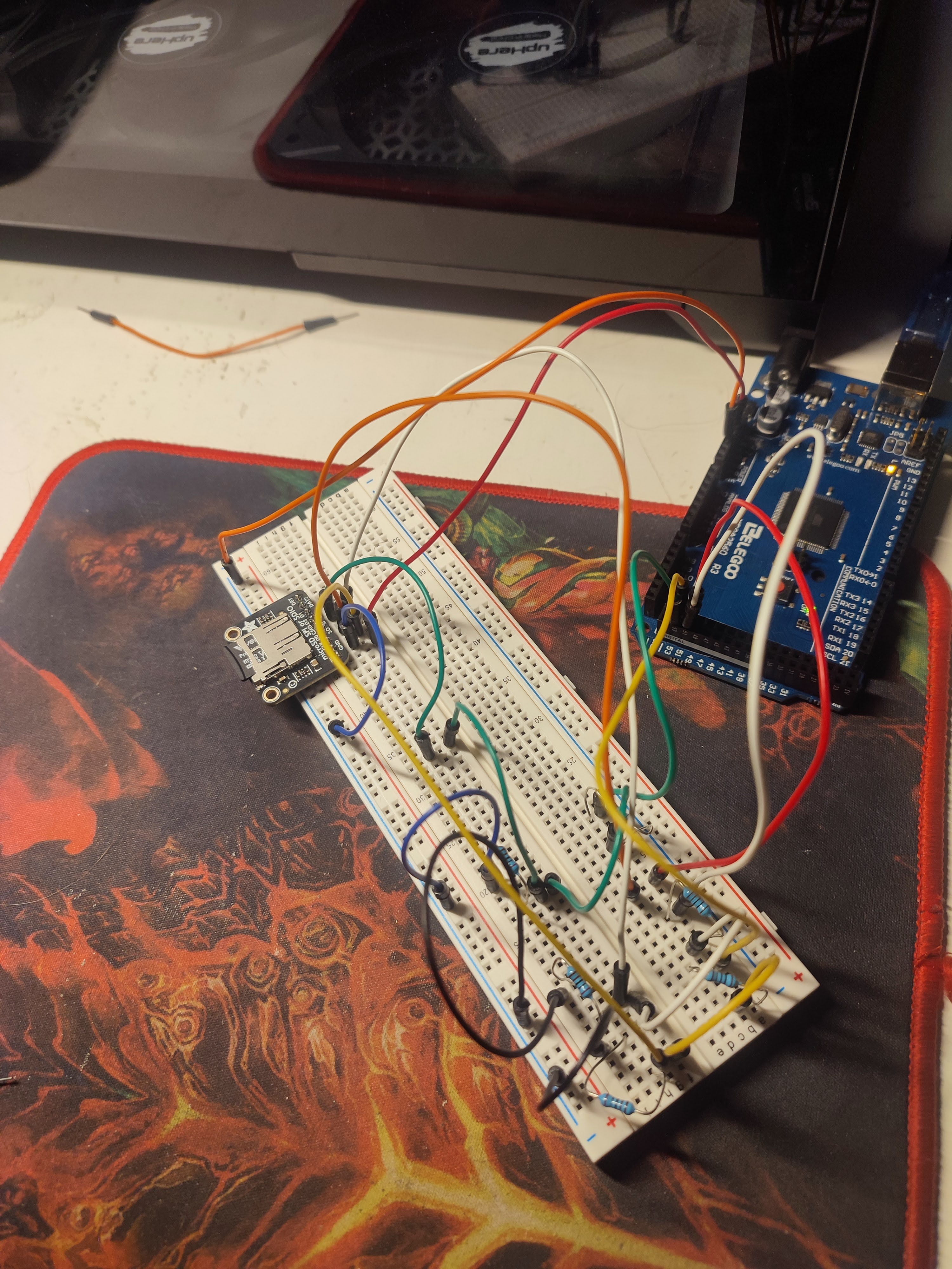
Once the new boards arrived a few days later I went to Uni and soldered up the pins and rung the bell for round two.
Confident that the board nor the SD card was the problem that only left one place, my verilog code. The thing is, running the testbench yielded a perfect result. Under simulation everything worked just as it should but reality had a different song to sing (Of course looking back this just meant that my testbench wasn't good enough). Countless hours make a tiny change, wait ages for the compiler to run, flash the board, and then wait in anticipation and start praying for a single response of 0x1 to confirm the SD card was in SPI mode.
It never happened. No matter what I tried I failed.
Running on the brink of near insanity I gave up and went to my course leader. He pulled out an ancient relic of the past, an oscilloscope coated in dust. He then and then proceeded to sit with me whilst probing the clock pins and data lines. We arrived at a consensus as to what the problem might of been. At this point it was quite late and I headed off to pub with a couple of mates. Then it was the weekend and all I could do was wait until Monday.
Monday came and it Easter break was over the lab was filled once more. This was the make or break day. If I couldn't get it to work today, I would admit defeat. After a few lectures I rushed to the lab and set everything up (being very careful to plug in the VCC and GND) compiled and flashed the new design and clicked run.
It worked. The SD card responded with 0x1 and now it worked I could finally begin the mountain of work which was creating the SD and the FAT drivers.